Vertical and MEMS probes micro-cutting for semiconductors testing industry
When it comes to the electronics industry, and specifically to the field of test equipment, high precision is essential. To achieve balance contact force, high current carrying capability and ultra-fine pitch to optimize wafer probe requirements, a high quality of the treated surfaces and the machined geometries of the vertical and MEMS probes is required. We are aware of these current and future requirements of the test equipment market.
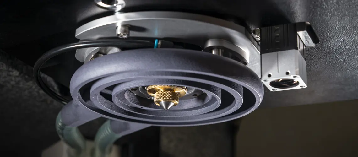
Vertical and MEMS probes µ-machining application overview
Advanced probe cards consist of thousands of vertical or MEMS probes for testing memory (DRAM, NAND) and non-memory (SoC) microprocessors on a wafer level.
MEMS probes, short for Micro-Electro-Mechanical Systems probes, are tiny devices that combine microelectronics and mechanical components. They are used to measure, sense, or interact with their surroundings at a microscale level. MEMS probes have applications in various fields, including electronics testing, biomedical sensing, and nanotechnology research.
A high quality vertical and MEMS probes micro-cutting is the foundation for achieving excellent reliability of quality testing, and technology scalability to address a broad range of testing requirements.
Vertical and MEMS Probes micro-machining achievements


Achieved results
We achieve high-precision vertical and MEMS probes micro-cutting in a wide range of materials like copper, palladium, irridium and other precious metals alloys. With foil thicknesses between 25-100 µm, we achieve cutting width down to 20 µm or even less, with a size accuracy < ± 2 μm.
With the capacity to produce any probe length, there is a remarkable flexibility in crafting all kinds of shapes and geometries, showcasing the adaptability and precision of high-tech machining methodologies.
You currently have a vertical probes or MEMS probes micro-machining project and you would like to know more about what we could achieve together?
Give us some more details!
The FEMTOsecond LASER technology is a perfect match for all industries requiring the highest precision without compromising quality and productivity.
Miniaturized components are used in all kind of devices. Several applications – e.g. in the electronics or MedTech world – are not imaginable without very small and tiny parts. Thus, this requires new ways to produce and manufacture these parts. With FEMTO LASER μ-machining there are various processes possible like drilling, cutting and turning. It's compatible with almost all materials that are otherwise very difficult to machine with conventional tools.
With each FEMTOsecond LASER pulse that hits the work-piece, a small amount of material immediately vaporizes. The material removal occurs in a controlled manner leading to no damage, burrs or any negative influences to the material integrity.
Your benefits:
- FEMTOsecond Laser source < 300 fs
- Highest level of accuracy and productivity
- Stable and repeatable quality
- Cold ablation keeping material integrity (no HAZ)
- Proven performance in 24/7 industrial environment

FEMTOsecond LASER machines provide advanced µ-machining solutions for high-tech production. It ensures impeccable surface smoothness and precise machining without thermal residue.
Other applications that might be interesting for you

Turning of contacts pins for IC substrates testing industry
Turning of contact pins (wires, bars and tubes) for semiconductors testing industry
Drilling and routing of composites and non-ferrous materials for printed circuit boards (PCB) industry
Let’s discuss your micro-machining operations
If you are looking for a high-tech production system as well as a partner to process state-of-the-art micro-machining, you are in the right place.